BY PEET VAN BILJON

The CHIPS and Science Act of 2022 injects $280 billion into U.S. research, innovation, and manufacturing over the next five years. The “CHIPS” name reflects the priority given to the semiconductor industry with $52.7 billion of dedicated semiconductor spending, including $39 billion in grants and a 25% tax credit for on-shore US manufacturing. The policy goal is to increase the U.S. manufacturing share of this crucial technology after years of decline – from 37 percent in 1990 to 12 percent (relative to the US semiconductor consumption of 34%) – mostly due to more aggressive industry investments by other governments. The Act also reflects the urgency of addressing semiconductor shortages and cyclic dynamics which trouble multiple industries (for example, automotive manufacturing), and impede U.S. economic growth.
The Importance of Semiconductors
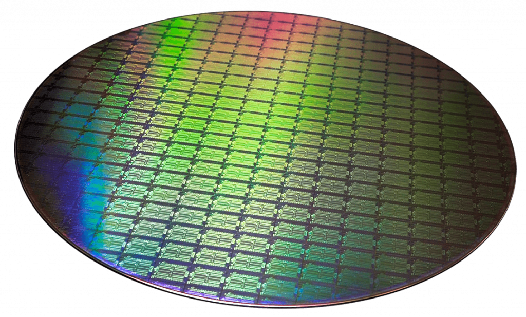
Our modern economy runs on semiconductors: both discrete devices such as power transistors and diodes that handle electric power or govern electric motors, and integrated circuits (ICs or “chips”) which are typically manufactured as wafers and contain thousands to billions of devices, mainly transistors. ICs may be microprocessors or memory chips used in computing, or commodity electronic building blocks used in a myriad of circuit designs, as well as custom circuits on a single chip, such as 5G wireless or GPS chips for your smartphone. An exponential growth in chip complexity over the last few decades has enabled our digital age and so much of the functionality we too easily take for granted. The smartphone in your pocket has far more computing power than NASA used for 1969 Apollo moon mission.
The global semiconductor market is forecast to be worth $633 billion in 2022, up 13.9 percent from 2021 of which the U.S. market share is about half. After a period of low profitability in the early 2000s, semiconductor companies have seen their economic profits grow strongly into the double digits since the late 2010s. The industry outlook is strong with no sign of demand abating. This makes some question why large industry subsidies are needed.

Industrial Policy Revisited
Though the CHIPS Act passed with bipartisan majorities in both the Senate and House, most Republicans opposed it. This is in line with a long tradition of skepticism about the U.S. government’s role in shaping and subsidizing industries. Unlike many other developed countries, the United States has generally eschewed an industrial policy of deliberately building up strategic industries. Yet, it also has a long tradition of making exceptions considered to be in the national interest.
The exigencies of World War II forced the U.S. government to be directly involved in weapons development, from basic research to production. The Manhattan Project (nuclear bomb) is the most famous example, but radar and computers were wartime government projects too. In each case, the government partnered with select universities and private firms. After the war, the government initially resolved to limit itself to only funding basic research. But the 1957 Sputnik launch and the military threat posed by the Soviet Union soon changed that, leading to the creation of NASA and DARPA in 1958. Technologies created with defense dollars have subsequently enabled great private-sector innovation, for example the internet and GPS. DARPA maintains partnerships with semiconductor firms for the development of new technologies, often with both military and civilian applications.
Policy Objectives
What is the public-policy rationale for a $52.7 billion government investment in one industry?
First, there is a substantial U.S. national-security interest, which includes self-sufficiency in advanced devices for defense and aerospace systems. Specifically, China’s territorial claims on Taiwan, which dominates global semiconductor manufacturing, is seen as a national-security risk.
Second, there is a desire to increase industry resilience to global supply-chain disruptions such as happened due to COVID lockdowns. A reliable supply of semiconductors is needed to make anything from home appliances and automobiles to the computers and data centers essential for continued national productivity growth.
Third, there is a global manufacturing capacity shortfall in the industry with factories running at full capacity, but unable to meet demand; backlogs are running at six months or longer.
Fourth, semiconductors are a top 5 U.S. export amounting to $60 billion, and a category in which the United States maintains a trade surplus.
Understanding more about the development and state of the semiconductor industry will provide further context on why the semiconductor industry was considered worthy of an exception to the general avoidance of industrial policy.

Semiconductor Developments
Transistors are tiny multilayered devices made from silicon or germanium of which some parts are precisely infused with impurities, enabling them to amplify or switch electrical current. Transistors and other semiconductors are the active components in almost all modern electronics. The transistor was invented by Bell Labs scientists in 1947 and the first integrated circuits (ICs) containing multiple transistors on a single chip appeared in the 1950s. In 1965, Gordon Moore (a future cofounder of Intel) wrote a prescient paper predicting that ICs containing more integrated electronics would revolutionize telecommunications and computing. Moore’s observation that the number of transistors on a single chip were doubling every two years as techniques improve became known as Moore’s Law, and was soon interpreted to mean that computing power would double every two years. In 1965 only 60 transistors fit on one IC, but Moore’s Law meant that by 1975 a state-of-the-art microchip would contain 65,000 transistors, which came to pass in 1975 exactly as predicted. Moore’s Law subsequently set industry expectations and became a self-fulfilling prophesy. By 1989, Intel launched the first 1-million-transistor microprocessor, the 80486. Today, over 2 trillion transistors can be crammed onto a chip. The end of Moore’s Law has been declared many times as miniaturization techniques ran into physical limits, yet ingenuous chip designers keep inventing new techniques to extend it.
The semiconductor node size in nanometers (nm) historically represented the smallest features that could be created by a particular manufacturing process. The node size is an indicator of how many devices one chip can contain (the smaller the node, the more devices) and hence related to Moore’s Law. Node size is also used to indicate the technology generation, with successive generations having smaller node sizes. The current cutting-edge node, 5 nm, is used for chips with the highest transistor densities such as powerful processors for mobile phones and computers. But as nodes advance, manufacturing and design costs escalate. Fabs, as individual factories are called, need new equipment to build different nodes. Building a 7nm or 5nm fab is so expensive that only Intel, TSMC, and Samsung have done so. These firms are now launching 3 nm processes.
However, most chip applications do not require the smallest nodes. Production of chips continue in nodes as large as 130 nm, while 20, 14 and 12 nm nodes can still meet support high-performance applications as process advances continue to be made by companies such as GlobalFoundries. There is a misperception that sub-7nm logic chip technology – still less than 30 percent of the market – is all-important. The United States needs to onshore a much broader set of semiconductor technologies. Such technologies include radio and optical communication chips used in a vast number of products essential for national security and industry resilience. Leading-edge innovation in these technologies depends more on specific device and circuit architectures, and less on node size.
Little is gained if American-made wafers have to shipped offshore to be packaged into devices. Chip packaging – historically a low-margin business – is now a critical technology as 2.5D and 3D architectures are needed for advanced designs. The CHIPS Act accordingly invests in microelectronics packaging technology with the new Advanced Packaging National Manufacturing Institute created by the Act.

The Current State of The Industry
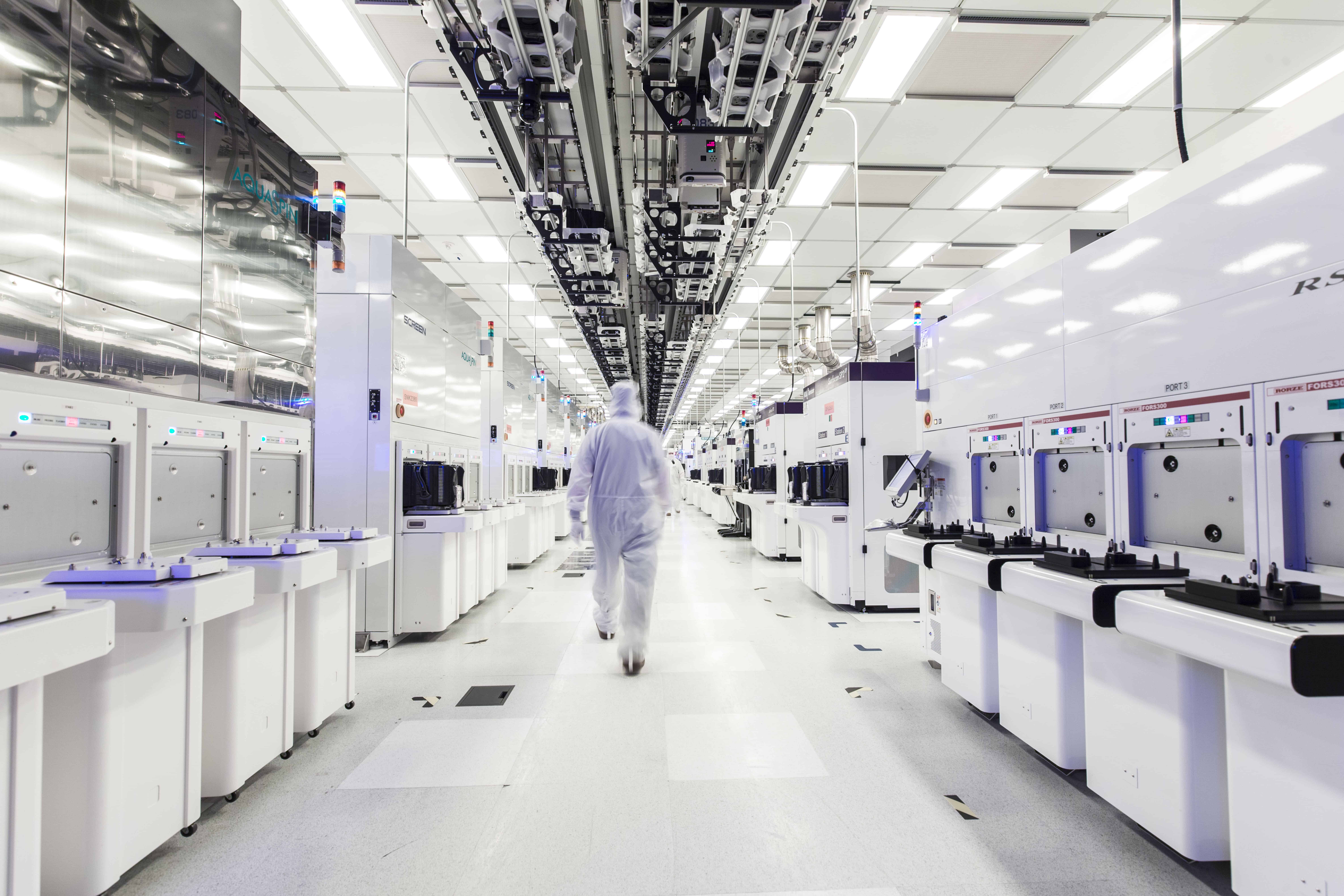
The industry is global and interconnected with three main types of semiconductor companies: those who design but do not manufacture are called “fabless” firms; those who only manufacture, usually for multiple design clients, are called foundries; and those who package and test the semiconductors coming out of the foundries. Increasing foundry capacity is costly with a new fab’s construction and operating costs easily being $2 -3 billion; more for the latest technologies. Chipmaking is a highly capital-intensive industry with each node generation demanding a larger expenditure on equipment than the previous. Due to high fixed costs, most chip companies outsource manufacturing to foundries, who achieve high utilization by making chips for multiple customers. AMD, Nvidia, and Qualcomm are all fabless: their chips are manufactured by contract foundries. Intel is one of the few remaining Integrated Device Manufacturers (DMs) – designers with their own foundries – as is Samsung. But even IDMs use contract foundries to make some of their chips.
The majority of semiconductors worldwide, including the most advanced chips with the highest component densities, are made in Taiwan by various foundries including the world’s largest, TSMC, which counts Apple, Qualcomm, Nvidia, and other technology companies among its clients. The next largest manufacturer is Samsung in South Korea.
Both TSMC and Samsung plan to build foundries in the United States: a $12 billion Arizona fab for TSMC, and a $17 billion fab in Texas for Samsung. Intel has started construction of its new $20 billion Arizona fabs and will also build new fabs in Ohio for an initial $20 billion investment which could grow to $100 billion making it the world’s largest chip plant. Several of these investments were contingent on the CHIPs Act passing. And just after the Act was signed by President Biden, Micron announced a $40 billion investment in U.S. memory chip manufacturing.
The CHIPS Act seems to be off to a good start.
All images courtesy of GlobalFoundries.
A different version of this post first appeared on De Gruyter Conversations.